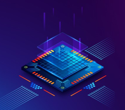
Moore’s Law vs. More than Moore: What’s Next for Semiconductor Scaling?
Written by - Ashwini H, from Abhiyantha Sept 30, 2024 5 Minutes

For decades, Moore’s Law has been the driving force behind the semiconductor industry, predicting that the number of transistors on a chip would double approximately every two years. This exponential growth in computing power has enabled the development of faster, smaller, and more efficient devices, from personal computers to smartphones. However, as we approach the physical limits of silicon-based technologies, Moore’s Law is facing significant challenges, and its pace has slowed.
The Limits of Moore’s Law
As transistors shrink below 5nm, several technical challenges emerge:
1. Quantum Tunneling: At atomic scales, electrons can "tunnel" through insulating layers, causing leakage currents and reducing the efficiency of transistors.
2. Heat Dissipation: Packing more transistors into smaller spaces increases heat, which is harder to manage, especially in compact devices
3. Manufacturing Costs: The costs of developing and manufacturing chips at sub-5nm nodes have skyrocketed, making it less economically viable for many applications.
While some further scaling may be possible with advanced lithography techniques like extreme ultraviolet (EUV) lithography, the benefits of shrinking transistors are diminishing, and the industry is looking for new ways to continue improving chip performance.
The Rise of “More than Moore”
Enter More than Moore, a concept that focuses on system-level innovations rather than solely relying on transistor miniaturization. More than Moore includes:
1. Heterogeneous Integration: Combining different types of processors (such as CPUs, GPUs, and AI accelerators) in a single package to optimize for specific tasks. This allows for greater flexibility and performance without shrinking transistors.
2. 3D Integration and Advanced Packaging: Instead of making chips smaller, manufacturers are stacking multiple layers of circuits vertically (3D ICs) and using advanced packaging technologies to enhance performance and power efficiency.
3. New Materials: Beyond silicon, materials like graphene, carbon nanotubes, and 2D materials are being explored to overcome the physical limitations of current technology.
4. Specialized Architectures: As general-purpose processors hit performance limits, domain-specific architectures (e.g., AI accelerators, neuromorphic computing) are being developed to handle specialized tasks more efficiently.
The Future of Semiconductor Scaling
While the era of easy transistor scaling is coming to an end, the combination of Moore’s Law and More than Moore presents exciting opportunities. Advanced system integration, new materials, and specialized designs are shaping the future of semiconductor technology, enabling breakthroughs in AI, 5G, quantum computing, and more.
In the end, the future of semiconductor innovation lies not just in shrinking transistors but in thinking bigger, focusing on how to integrate diverse technologies into more powerful, efficient systems.
Share This Blogs
Featured Blogs

Top 10+ Most Asked VLSI Interview Questions with Answers by Industry Expert
The Ultimate Guide to Finding the Best VLSI Course in Bangalore
A Comprehensive Guide to Securing Your Dream Job in the Semiconductor Industry

Advancements in Semiconductor Manufacturing: Pioneering the Future of Electronics

From Classrooms to Cleanrooms: Academia's Role in Shaping India’s Semiconductor Industry

The Evolution of Integrated Circuits: A Journey of Innovation

How to Learn VLSI from Scratch

Will AI disrupt EDA? Let’s examine the future of semiconductor design with AI.
Understanding FinFET Technology: A Comprehensive Overview.

Common Challenges in Designing Low-Power VLSI Circuits