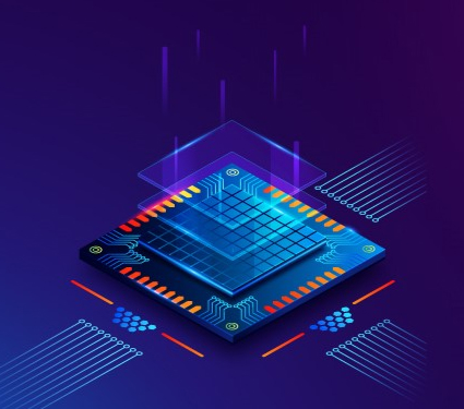
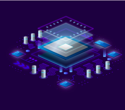
Will AI disrupt EDA? Let’s examine the future of semiconductor design with AI.
Written by Dr. Mamidi Nagaraju, from Abhiyantha July 31, 2024 5 Minutes

The rise of Artificial Intelligence (AI) in various industries has sparked discussions about its potential to revolutionise Electronic Design Automation (EDA). AI's ability to process large datasets and identify patterns offers significant benefits for semiconductor design, presenting a new era of efficiency and innovation.
AI's Role in EDA
1. Automation and Efficiency:
AI can automate repetitive and time-consuming tasks in the EDA workflow. For instance, layout generation, verification, and optimisation can be streamlined using machine learning. algorithms. This automation not only speeds up the design process but also reduces the likelihood of human errors, leading to more reliable and accurate designs.
2. Enhanced Design Quality:
AI algorithms can analyse vast amounts of design data to identify potential issues early in the design phase. Predictive analytics can foresee problems that might arise during manufacturing. or operation, allowing engineers to address these issues proactively. This predictive capability enhances the overall quality and robustness of the final product.
3. Optimisation:
AI-driven tools can optimise various aspects of semiconductor design, such as power consumption, performance, and area (PPA). By continuously learning from previous designs, AI can suggest improvements and alternatives that might not be apparent through traditional methods. This leads to more efficient and effective designs.
Challenges in Integrating AI with EDA
1. Data Management:
The success of AI in EDA relies heavily on the availability and quality of data. Semiconductor designs generate massive amounts of data, and managing this data effectively is crucial. Ensuring that AI algorithms have access to accurate and relevant data is a significant challenge that needs to addressed.
2. Expertise and Integration:
Integrating AI into existing EDA workflows requires specialised knowledge in both AI and semiconductor design. Engineers need to be trained in AI techniques and tools and collaboration. between AI specialists and EDA experts is essential. Bridging this knowledge gap is vital for the successful implementation of AI in EDA.
3. Trust and Reliability:
AI algorithms are often seen as "black boxes" due to their complexity and lack of transparency. Building trust in AI-driven EDA tools requires thorough validation and testing to ensure their reliability. Engineers need to understand how AI makes decisions and be confident in the accuracy and dependability of the results.
The Future of EDA with AI
The integration of AI into EDA is still in its early stages, but the potential benefits are substantial. As AI technology continues to evolve, it is expected to play an increasingly important role in semiconductor design. Companies that embrace AI-driven EDA tools will likely gain a competitive edge by reducing design cycles, improving quality, and fostering innovation.
In conclusion, AI has the potential to disrupt the EDA landscape significantly. While challenges remain, the ongoing advancements in AI and machine learning offer promising opportunities for enhancing semiconductor design processes. The future of EDA with AI is bright, and its successful integration could lead to unprecedented levels of efficiency and innovation in the semiconductor industry.
For more insights and detailed discussions on this topic, you can visit the full article below for reference:https://semiengineering.com/will-ai-disrupt-eda/
Share This Blogs
Featured Blogs

Top 10+ Most Asked VLSI Interview Questions with Answers by Industry Expert
The Ultimate Guide to Finding the Best VLSI Course in Bangalore
A Comprehensive Guide to Securing Your Dream Job in the Semiconductor Industry
Advancements in Semiconductor Manufacturing: Pioneering the Future of Electronics
Embracing the Future: Advanced Node Technologies in VLSI Design
From Classrooms to Cleanrooms: Academia's Role in Shaping India’s Semiconductor Industry

The Evolution of Integrated Circuits: A Journey of Innovation

How to Learn VLSI from Scratch
Breaking Boundaries with Chiplets: The Future of Advanced Packaging.
Understanding FinFET Technology: A Comprehensive Overview.
Moore’s Law vs. More than Moore: What’s Next for Semiconductor Scaling?
Common Challenges in Designing Low-Power VLSI Circuits