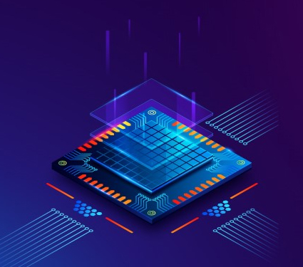
Common Challenges in Designing Low-Power VLSI Circuits
Written by - Ashwini H, from Abhiyantha November 22, 2024 5 Minutes

In today's technology-driven world, low-power VLSI design is crucial for enabling portable devices, IoT gadgets, and energy-efficient computing systems. As the demand for lower power consumption continues to grow, designers face a range of challenges that require innovative solutions and trade-offs. This article highlights the common issues encountered when designing low-power VLSI circuits and provides insights into overcoming them.
Power Dissipation: The Core Challenge
Power dissipation, the product of total current and voltage loss in a circuit, is a key constraint in low-power VLSI design, especially when it comes to portable devices. As device portability increases, power dissipation must be carefully managed.
Key Reasons for Power Management in VLSI
- Costs associated with packaging and cooling
- Standby time and battery life
- Digital noise immunity
- Environmental concerns
1. Balancing Power, Performance, and Area (PPA)
Designing for low power often requires compromises between power, performance, and area (PPA). Reducing power by lowering supply voltage can slow transistor switching speeds, impacting performance. Techniques like clock gating and multi-threshold voltage designs may increase area or complexity, making optimization a delicate balancing act.
2. Managing Dynamic Power
Dynamic power, caused by switching activities and capacitive charging, dominates active circuits. High switching frequencies in modern chips exacerbate power dissipation. Effective techniques like clock gating help minimize switching activity and reduce dynamic power consumption.
3. Controlling Leakage Power
At advanced technology nodes, leakage power, especially during standby, becomes a significant challenge. Subthreshold leakage and gate oxide tunneling increase with shrinking dimensions. Power gating and multi-threshold CMOS (MTCMOS) technologies help address this, although they introduce additional design complexity.
4. Power Delivery and IR Drop
Efficient power delivery across chips while maintaining stable voltage levels is critical, particularly in low-power designs with reduced supply voltages. IR drop and noise are significant concerns, but hierarchical power delivery networks and decoupling capacitors can help mitigate these challenges.
5. Thermal Management
Even low-power designs can generate localized heat that degrades reliability. Thermal management is essential through thermal-aware placement and dynamic power throttling to prevent hotspots and maintain circuit performance.
6. Memory Power Optimization
Memory components, such as SRAM and DRAM, contribute significantly to power consumption due to frequent read/write operations. Techniques like power-gated SRAM and efficient memory architectures address both dynamic power and leakage power challenges in memory subsystems.
7. Process Variations and Reliability
At nanoscale nodes, process variations affect transistor characteristics and complicate power optimization. Techniques like statistical timing analysis and adaptive voltage scaling are crucial for ensuring robust, reliable low-power VLSI designs.
8. Testability in Low-Power Designs
Testing low-power circuits presents unique challenges, as Design for Test (DFT) techniques can increase power consumption. Power-aware testing strategies, such as clock gating in test mode and segmented scan chains, help minimize test power while ensuring proper functionality.
Conclusion
Designing low-power VLSI circuits requires a holistic approach to power management while maintaining performance and area constraints. By adopting innovative techniques like Dynamic Voltage and Frequency Scaling (DVFS), power gating, and thermal-aware design strategies, engineers can overcome these challenges and deliver energy-efficient chips that meet the growing demands for sustainable technology.
Low-power VLSI design is no longer just a goal but a necessity for powering the next generation of devices and systems.
Share This Blogs
Featured Blogs

Top 10+ Most Asked VLSI Interview Questions with Answers by Industry Expert
The Ultimate Guide to Finding the Best VLSI Course in Bangalore
A Comprehensive Guide to Securing Your Dream Job in the Semiconductor Industry
Advancements in Semiconductor Manufacturing: Pioneering the Future of Electronics

Embracing the Future: Advanced Node Technologies in VLSI Design
From Classrooms to Cleanrooms: Academia's Role in Shaping India’s Semiconductor Industry

The Evolution of Integrated Circuits: A Journey of Innovation

Will AI disrupt EDA? Let’s examine the future of semiconductor design with AI.

Breaking Boundaries with Chiplets: The Future of Advanced Packaging.

Moore’s Law vs. More than Moore: What’s Next for Semiconductor Scaling?