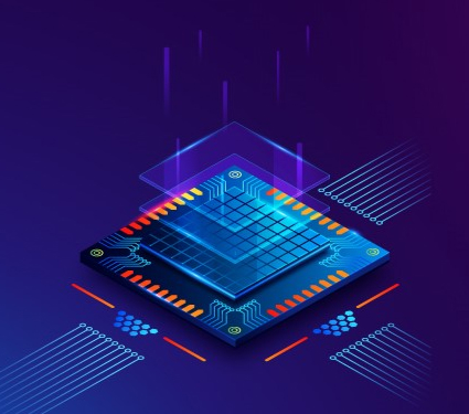
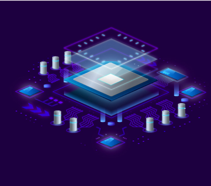
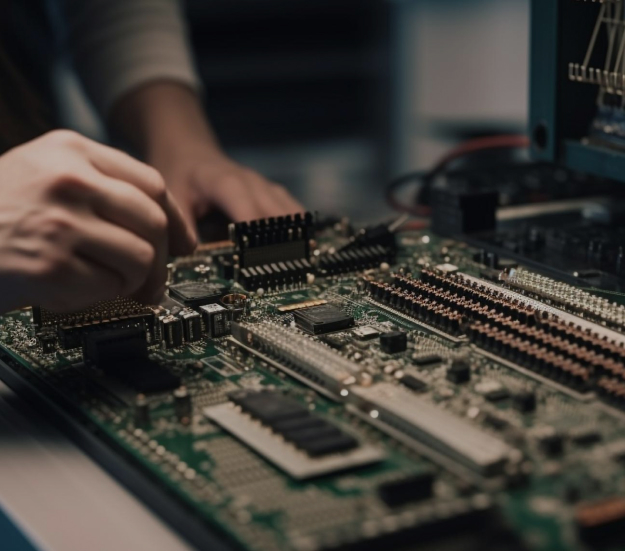
Breaking Boundaries with Chiplets: The Future of Advanced Packaging
Written by - Ashwini H, from Abhiyantha Sept 26, 2024 5 Minutes

As Moore’s Law slows down and transistor miniaturization reaches its physical limits, the semiconductor industry is shifting focus towards advanced packaging techniques to continue pushing the boundaries of performance. One of the most promising approaches in this space is chiplet-based design, which is revolutionizing how chips are integrated and manufactured.
What Are Chiplets?
Chiplets are small, modular components that can be combined to form a more complex system-on-chip (SoC). Instead of designing and manufacturing a single monolithic chip, chiplet-based architectures allow different functions, such as CPUs, GPUs, and memory, to be built as individual modules. These chiplets are then interconnected within a single package using high-speed interconnects.
This modular approach offers several key advantages:
1. Increased Flexibility:
Chiplets allow designers to mix and match components from different process nodes. For example, a CPU can be built on an advanced 5nm process, while memory or other components can be made using more mature, cost-effective nodes. This flexibility reduces costs while optimizing performance.
2. Improved Yield:
Manufacturing large monolithic chips increases the risk of defects, leading to lower yields and higher costs. With chiplets, smaller modules are easier to produce with higher yields, and defective modules can be replaced without scrapping an entire chip.
3. Customizability:
Chiplets provide a path to creating customized solutions for different applications. Companies can tailor chiplets to specific workloads, such as AI, cloud computing, or 5G, by adding or swapping specific modules based on their needs.
Key Advanced Packaging Techniques for Chiplets
1. 2.5D and 3D Packaging:
In 2.5D packaging, chiplets are placed side by side on a silicon interposer, which allows them to communicate with high bandwidth and low latency. 3D packaging goes a step further by stacking chiplets vertically, which reduces footprint and shortens interconnect distances, further improving performance.
2. Interconnect Technologies
Technologies like silicon bridges and through-silicon vias (TSVs) enable fast, power-efficient communication between chiplets, mimicking the seamless connectivity of a monolithic design
3. Heterogeneous Integration
Chiplets allow for heterogeneous integration, where different types of computing units (CPU, GPU, AI accelerators) and memory can be packed into a single package. This approach is highly efficient for applications requiring diverse processing workloads.
Opportunities and Applications
Chiplet-based architectures are already being adopted by industry leaders. AMD, for example, has successfully used chiplet designs in its EPYC and Ryzen processors, achieving higher core counts and better performance scalability than traditional monolithic chips. Similarly, Intel’s Foveros and EMIB technologies enable advanced packaging for chiplets, facilitating high-performance computing and AI applications.
The data center and high-performance computing (HPC) industries are among the biggest beneficiaries of chiplet technology, where scalability and power efficiency are critical. However, chiplets are also poised to transform consumer electronics, automotive systems, and IoT devices by providing customized, cost-effective solutions that deliver cutting-edge performance.
Conclusion
As the semiconductor industry moves beyond traditional scaling, chiplets are emerging as a powerful solution for overcoming the challenges of Moore’s Law. By enabling modularity, flexibility, and customizability, chiplets are opening new frontiers in advanced packaging and unlocking the potential for next-generation applications across various industries. As this technology matures, we can expect chiplet-based architectures to become a cornerstone of semiconductor innovation.
Share This Blogs
Featured Blogs

Top 10+ Most Asked VLSI Interview Questions with Answers by Industry Expert
The Ultimate Guide to Finding the Best VLSI Course in Bangalore
A Comprehensive Guide to Securing Your Dream Job in the Semiconductor Industry
Advancements in Semiconductor Manufacturing: Pioneering the Future of Electronics
From Classrooms to Cleanrooms: Academia's Role in Shaping India’s Semiconductor Industry
The Evolution of Integrated Circuits: A Journey of Innovation

How to Learn VLSI from Scratch

Will AI disrupt EDA? Let’s examine the future of semiconductor design with AI.
Understanding FinFET Technology: A Comprehensive Overview.
Moore’s Law vs. More than Moore: What’s Next for Semiconductor Scaling?
Common Challenges in Designing Low-Power VLSI Circuits