Understanding FinFET Technology: A Comprehensive Overview
Written by - Pooja C, from Abhiyantha sept 30, 2024 5 Minutes
In the fast-paced world of semiconductor technology, FinFET (Fin Field-Effect Transistor) represents a groundbreaking advancement. This blog explores FinFET technology, its importance, and how it differs from traditional MOSFETs in integrated circuit (IC) design.
What is FinFET Technology?
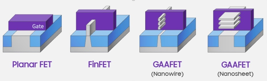
FinFET, short for Fin Field-Effect Transistor, is an innovative 3D transistor structure that enhances traditional planar transistor designs. Unlike conventional MOSFETs, where the gate electrode is laid flat over the semiconductor channel, FinFETs use a vertical "fin" structure that protrudes from the substrate. This 3D design improves the control over the flow of electrons and boosts the transistor's performance.
Evolution from Planar to FinFET
Historically, as semiconductor devices shrank in size to meet the demands for higher performance and lower power consumption, the planar transistor design began to face significant limitations. Scaling down planar transistors led to issues like leakage current and insufficient gate control, which hampered performance and efficiency.
FinFET technology emerged as a solution to these challenges. By creating a three-dimensional structure where the gate surrounds the channel on three sides, FinFETs offer superior electrostatic control compared to their planar counterparts. This increased control translates to lower leakage currents, reduced power consumption, and improved performance.
MOSFET vs. FinFET: Key Differences
1. Structure and Gate Control
MOSFET (Metal-Oxide-Semiconductor Field-Effect Transistor): Traditional MOSFETs feature a planar design where the gate is positioned flat on top of the semiconductor channel. This configuration controls current flow by modulating the channel's conductivity through an electric field.
FinFET: In FinFETs, the semiconductor channel is created as a thin vertical "fin" with the gate wrapping around it on three sides. This 3D structure provides better electrostatic control, reducing leakage currents and mitigating short-channel effects.
2. Performance and Scaling
MOSFET: As the size of MOSFETs decreases, maintaining effective control over the channel becomes increasingly difficult. This leads to performance degradation, increased leakage currents, and higher power consumption.
FinFET: The 3D gate structure of FinFETs allows for superior electrostatic control even at smaller transistor nodes. This leads to enhanced performance, higher drive currents, and reduced power consumption compared to planar MOSFETs.
3. Power Efficiency
MOSFET: In smaller nodes, traditional MOSFETs suffer from increased leakage currents and power dissipation, which can be detrimental to battery-operated and power-sensitive applications.
FinFET: FinFETs effectively reduce leakage currents and power consumption due to their advanced gate control, making them ideal for power-efficient and mobile applications.
4. Manufacturing Complexity
MOSFET: The planar design of MOSFETs simplifies manufacturing processes, making them easier to fabricate compared to more complex 3D structures.
FinFET: The 3D nature of FinFETs introduces additional complexity in the fabrication process. However, this complexity is offset by the substantial performance and efficiency gains they provide.
Applications and Impact
FinFETs are essential in various high-performance computing applications, including processors, memory chips, and mobile devices. Their balance of performance and power efficiency makes them versatile for a wide range of electronics, from smartphones to servers.
Beyond individual devices, FinFET technology drives advancements in fields like artificial intelligence, data centers, and consumer electronics. By enabling more efficient and powerful chips, FinFETs meet the growing demand for sophisticated technology capable of handling complex tasks while remaining energy-efficient.
Future Prospects
As technology continues to advance, researchers are exploring further enhancements to FinFET technology, including the development of new materials and structures. Innovations such as Gate-All-Around (GAA) transistors are on the horizon, which promise even greater control and performance improvements. However, FinFET technology remains a key player in the semiconductor industry, providing a robust foundation for the continued evolution of electronic devices.
Conclusion
FinFET technology represents a significant leap forward in transistor design, addressing the limitations of planar MOSFETs and setting the stage for future advancements in electronics. Its ability to offer enhanced performance, lower power consumption, and scalability makes it a cornerstone of modern semiconductor technology. As the industry moves towards even more advanced technologies, FinFETs will continue to play a crucial role in shaping the future of electronics.
Share This Blogs
Featured Blogs

Top 10+ Most Asked VLSI Interview Questions with Answers by Industry Expert
The Ultimate Guide to Finding the Best VLSI Course in Bangalore
A Comprehensive Guide to Securing Your Dream Job in the Semiconductor Industry
Advancements in Semiconductor Manufacturing: Pioneering the Future of Electronics

Embracing the Future: Advanced Node Technologies in VLSI Design
From Classrooms to Cleanrooms: Academia's Role in Shaping India’s Semiconductor Industry

The Evolution of Integrated Circuits: A Journey of Innovation

Will AI disrupt EDA? Let’s examine the future of semiconductor design with AI.
Breaking Boundaries with Chiplets: The Future of Advanced Packaging.
Moore’s Law vs. More than Moore: What’s Next for Semiconductor Scaling?

Common Challenges in Designing Low-Power VLSI Circuits