Embracing the Future: Advanced Node Technologies in VLSI Design
Written by - Pooja C, from Abhiyantha July 31, 2024 5 Minutes

The realm of Very-Large-Scale Integration (VLSI) design has been transformative in shaping modern electronics. As technology progresses, the push for smaller, faster, and more efficient integrated circuits (ICs) has spurred the development of advanced node technologies. These technologies are not only expanding the limits of what’s achievable but also transforming our approach to VLSI design.
Key Technologies Driving Advanced Nodes
1. Extreme Ultraviolet Lithography (EUV):
EUV lithography is fundamental to modern semiconductor fabrication. Utilising light with an extremely short wavelength (13.5 nm), EUV lithography allows for the precise patterning of semiconductor wafers, enabling the production of smaller and more complex features. This technology is crucial for maintaining Moore’s Law and achieving continued performance improvements at advanced nodes.
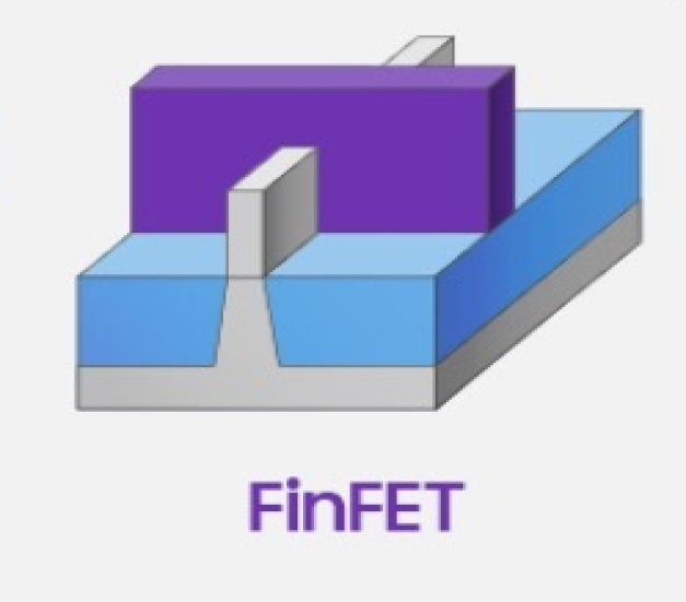
2. FinFET and Beyond:
FinFETs have revolutionised transistor design by providing better control over the transistor channel compared to traditional planar transistors. The next generation of transistor architectures, such as Gate-All-Around (GAA) FETs, is emerging. GAA FETs offer even greater performance and power efficiency by enhancing gate control over the transistor channel, pushing the boundaries of semiconductor technology further.
3. Advanced Materials:
The quest for smaller nodes has driven research into new materials beyond silicon. Materials like graphene and transition metal dichalcogenides (TMDs) are being explored for their superior electrical properties. These materials could lead to groundbreaking advancements by enabling the creation of smaller and more efficient devices, potentially transforming semiconductor technology.
4. 3D Integration:
To address the limitations of planar scaling, 3D integration technologies such as Through-Silicon Vias (TSVs) and monolithic 3D ICs are being developed. These techniques involve stacking multiple layers of chips, which can significantly increase density and performance while reducing power consumption and interconnect delays. 3D integration offers a path to overcoming the constraints of traditional 2D scaling.
5. Machine Learning and AI:
The design and optimisation processes for advanced nodes are increasingly leveraging artificial intelligence (AI) and machine learning (ML). These technologies assist in predicting performance, optimising layouts, and automating various design aspects. AI-driven tools are becoming essential for managing the complexity of modern VLSI designs, enabling faster and more accurate design cycles.
Challenges and Solutions
1. Physical Limitations:
As transistor sizes shrink, physical limitations such as quantum effects and increased leakage currents become more pronounced. Addressing these challenges requires innovative solutions in both materials and transistor designs. Research into new transistor architectures and materials is crucial for mitigating these issues and pushing technology forward.
2. Cost and Complexity:
Developing and deploying advanced node technologies comes with escalating costs. The complexity of manufacturing equipment and processes necessitates substantial investment. Collaborative efforts between industry stakeholders and the development of cost-effective solutions are essential to managing these financial and technical challenges.
3. Design Tools and Verification:
The increasing complexity of designs requires advanced design tools and verification methods. Ensuring that designs meet performance, power, and reliability standards demands sophisticated simulation and verification techniques. Integrating AI and ML into these tools is helping address the growing demands and complexities of modern VLSI designs.
The Future Outlook
The future of VLSI design is poised to be shaped by ongoing advancements in node technologies. As the industry moves towards nodes like 2nm and beyond, the focus will be on addressing the physical limitations of current technologies and exploring alternative materials and architectures.
AI and machine learning will play increasingly pivotal roles, driving innovation in design, manufacturing, and optimization. Additionally, the integration of 3D ICs and new materials will be crucial for overcoming the limitations of traditional scaling approaches.
In summary, embracing advanced node technologies in VLSI design is about more than just shrinking transistor sizes; it’s about reimagining what’s possible in electronic systems. While the challenges are significant, the potential rewards are vast.
As technology continues to evolve, the semiconductor industry will drive forward new breakthroughs that will transform various industries and enhance our daily lives.
By staying at the cutting edge of these advancements, the semiconductor sector will ensure that the future of electronics is bright and full of potential.
Share This Blogs
Featured Blogs

Top 10+ Most Asked VLSI Interview Questions with Answers by Industry Expert
The Ultimate Guide to Finding the Best VLSI Course in Bangalore

A Comprehensive Guide to Securing Your Dream Job in the Semiconductor Industry

Advancements in Semiconductor Manufacturing: Pioneering the Future of Electronics
From Classrooms to Cleanrooms: Academia's Role in Shaping India’s Semiconductor Industry

The Evolution of Integrated Circuits: A Journey of Innovation

How to Learn VLSI from Scratch

Will AI disrupt EDA? Let’s examine the future of semiconductor design with AI.

Breaking Boundaries with Chiplets: The Future of Advanced Packaging.
Understanding FinFET Technology: A Comprehensive Overview.

Moore’s Law vs. More than Moore: What’s Next for Semiconductor Scaling?

Common Challenges in Designing Low-Power VLSI Circuits