Back
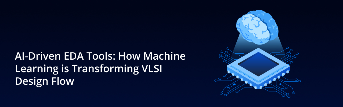
AI-Driven EDA Tools: How Machine Learning is Transforming VLSI Design Flow
Written by - Ashwini H, from Abhiyantha May 26, 2025 5 Minutes
The complexity of modern chip design has reached unprecedented levels, pushing the boundaries of traditional Electronic Design Automation (EDA) tools. With shrinking process nodes, increasing transistor counts, and tight power-performance- area (PPA) constraints, designers face growing challenges in achieving first-time silicon success. To address these demands, the VLSI industry is turning to Artificial Intelligence (AI) and Machine Learning (ML) — technologies that are redefining how design automation is approached across the entire VLSI design flow.
Why AI in EDA?
Traditional EDA tools rely heavily on rule-based heuristics, developed over decades of engineering expertise. While effective, these approaches often require significant manual intervention and fine-tuning. AI/ML introduces data-driven adaptability, enabling tools to learn from past designs and optimize processes in ways that were previously impractical or too time-consuming. With access to design history and performance feedback, AI models can predict outcomes, make intelligent decisions, and speed up convergence in complex flows.
Applications Across the VLSI Design Flow
1. RTL Design and Optimization
At the front-end, ML is being applied to analyze RTL code for design quality, potential bottlenecks, and synthesis readiness. By learning from prior RTL implementations and corresponding synthesis results, AI models can suggest architectural changes or code refactoring to improve timing or reduce area — optimizing RTL design with AI before synthesis begins.
2. Logic Synthesis and Mapping
AI-assisted synthesis engines are being trained to predict the most optimal technology mapping strategies for a given RTL, based on the characteristics of the target standard cell library. These predictions help reduce logic depth, switching activity, and area usage — contributing directly to improved PPA metrics and AI- based logic synthesis.
3. Floorplanning and Placement
Floorplanning and placement are two of the most time-consuming and PPA-critical stages of physical design. ML algorithms can quickly analyze billions of data points to recommend block placements, macro arrangements, or pin assignments that minimize congestion and improve routability. Reinforcement learning techniques are especially useful here, where models iteratively refine floorplans based on timing and area feedback. This AI-driven floorplanning optimization reduces manual effort significantly.
4. Power and Timing Optimization
AI is also playing a role in power estimation and reduction. Predictive models can estimate power hotspots and suggest design modifications or dynamic voltage/frequency scaling strategies. Similarly, ML can be used to predict timing violations and guide optimization paths for timing closure, reducing iteration time significantly — supporting AI for power-performance-area optimization.
5. Verification and Regression Analysis
Verification is another area where AI is making a strong impact. From functional simulation to formal verification, ML techniques are used to prioritize test vectors, detect unreachable states, and predict high-risk areas in the design. Natural Language Processing (NLP) is being explored to automatically generate assertions and extract intent from design documentation. These AI-powered EDA tools enhance verification productivity and accuracy.
The Road Ahead
AI integration into EDA is still evolving, but its trajectory is clear — enabling smarter, faster, and more autonomous design tools. While these AI-driven systems do not replace engineers, they serve as intelligent assistants, helping teams handle complexity, reduce iteration cycles, and accelerate time-to-market.
The fusion of AI and EDA represents a significant shift in how silicon will be designed in the coming decade. As these tools mature, we can expect a transformation in design productivity, innovation velocity, and ultimately, the chips that power our digital future.
Looking to dive deeper into the intersection of AI, machine learning, and EDA? Stay tuned to our blog or visit Abhiyantha for expert insights on VLSI and semiconductor design automation.
Share This Blogs
Featured Blogs

Top 10+ Most Asked VLSI Interview Questions with Answers by Industry Expert
The Ultimate Guide to Finding the Best VLSI Course in Bangalore

A Comprehensive Guide to Securing Your Dream Job in the Semiconductor Industry

Advancements in Semiconductor Manufacturing: Pioneering the Future of Electronics

Embracing the Future: Advanced Node Technologies in VLSI Design
From Classrooms to Cleanrooms: Academia's Role in Shaping India’s Semiconductor Industry
The Evolution of Integrated Circuits: A Journey of Innovation

Will AI disrupt EDA? Let’s examine the future of semiconductor design with AI.

Breaking Boundaries with Chiplets: The Future of Advanced Packaging.
Understanding FinFET Technology: A Comprehensive Overview.

Moore’s Law vs. More than Moore: What’s Next for Semiconductor Scaling?

Common Challenges in Designing Low-Power VLSI Circuits