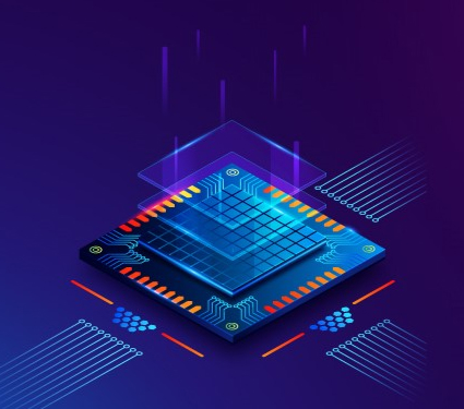
Challenges and Opportunities in 2nm and Beyond
Written by - Ashwini H From Abhiyantha Oct 22, 2024 5 Minutes

As the semiconductor industry pushes toward 2nm technology nodes and beyond, the challenges are becoming more complex than ever. The traditional scaling approach that has been driven by Moore’s Law is now facing serious limitations. Yet, these challenges also present unique opportunities for innovation and the continued advancement of the technology powering our digital world.
Challenges at 2nm and Beyond
1. Quantum Effects:
As transistors approach atomic scales, quantum tunneling becomes a significant issue. Electrons can pass through barriers meant to contain them, leading to leakage currents, increased power consumption, and potential reliability issues.
2. Heat Dissipation:
With billions of transistors packed into ever-smaller spaces, managing heat becomes extremely difficult. At such small scales, excess heat can damage circuits, reduce performance, and lead to faster wear-out of devices.
3. Manufacturing Costs:
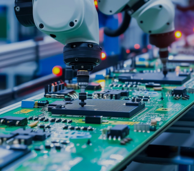
Building chips at 2nm requires cutting-edge technologies like extreme ultraviolet (EUV) lithography, which is incredibly expensive. Fabs capable of producing 2nm chips cost billions of dollars to build, pushing up development and production costs.
4. Material Limitations:
Traditional silicon is reaching its physical limits in terms of scaling. As devices shrink, it becomes more difficult for silicon to maintain performance and efficiency, making it necessary to explore new materials.
Opportunities for Innovation
1. New Materials:
As silicon reaches its limitations, new materials like graphene, carbon nanotubes, and 2D materials (such as transition metal dichalcogenides) are being explored to replace or complement silicon in next-generation transistors. These materials offer higher electron mobility, potentially overcoming current limitations.
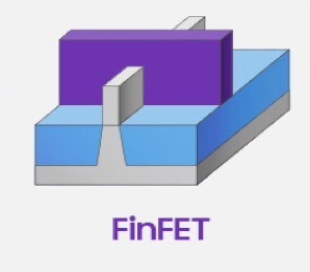
2. Advanced Transistor Designs:
Innovations like Gate-All-Around (GAA) and nanowire transistors offer better control over electron flow, improving performance and reducing power consumption at advanced nodes. These designs are key to continuing scaling beyond 2nm.
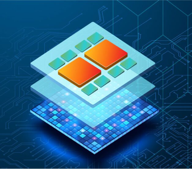
3. 3D Stacking:
3D Integrated Circuits (3D ICs) and advanced packaging techniques like chiplets and heterogeneous integration are becoming crucial as horizontal scaling slows down. By stacking chips vertically and integrating different components into a single package, manufacturers can enhance performance, reduce latency, and increase functionality without further shrinking individual transistors.
4. AI and Specialized Computing:
The demand for AI, machine learning, and specialized accelerators is driving new opportunities in chip design. Instead of relying purely on general-purpose processors, domain-specific architectures tailored for AI and high- performance computing (HPC) workloads can offer significant performance boosts without needing to shrink transistor size further.
The Road Ahead
The transition to 2nm and beyond will undoubtedly be challenging, but the semiconductor industry has a long history of overcoming technical hurdles through innovation. While the days of easy scaling may be behind us, the convergence of new materials, 3D architectures, and domain-specific designs offers a promising path forward. By embracing these opportunities, the industry can continue to deliver more powerful and efficient chips that will fuel the next generation of technology.
Share This Blogs
Featured Blogs

Top 10+ Most Asked VLSI Interview Questions with Answers by Industry Expert
The Ultimate Guide to Finding the Best VLSI Course in Bangalore
A Comprehensive Guide to Securing Your Dream Job in the Semiconductor Industry
Advancements in Semiconductor Manufacturing: Pioneering the Future of Electronics
Embracing the Future: Advanced Node Technologies in VLSI Design
From Classrooms to Cleanrooms: Academia's Role in Shaping India’s Semiconductor Industry

The Evolution of Integrated Circuits: A Journey of Innovation

How to Learn VLSI from Scratch

Will AI disrupt EDA? Let’s examine the future of semiconductor design with AI.
Breaking Boundaries with Chiplets: The Future of Advanced Packaging.
Understanding FinFET Technology: A Comprehensive Overview.

Moore’s Law vs. More than Moore: What’s Next for Semiconductor Scaling?

Common Challenges in Designing Low-Power VLSI Circuits